GPIO SS Peripheral Subsystem Architecture
About This Architecture
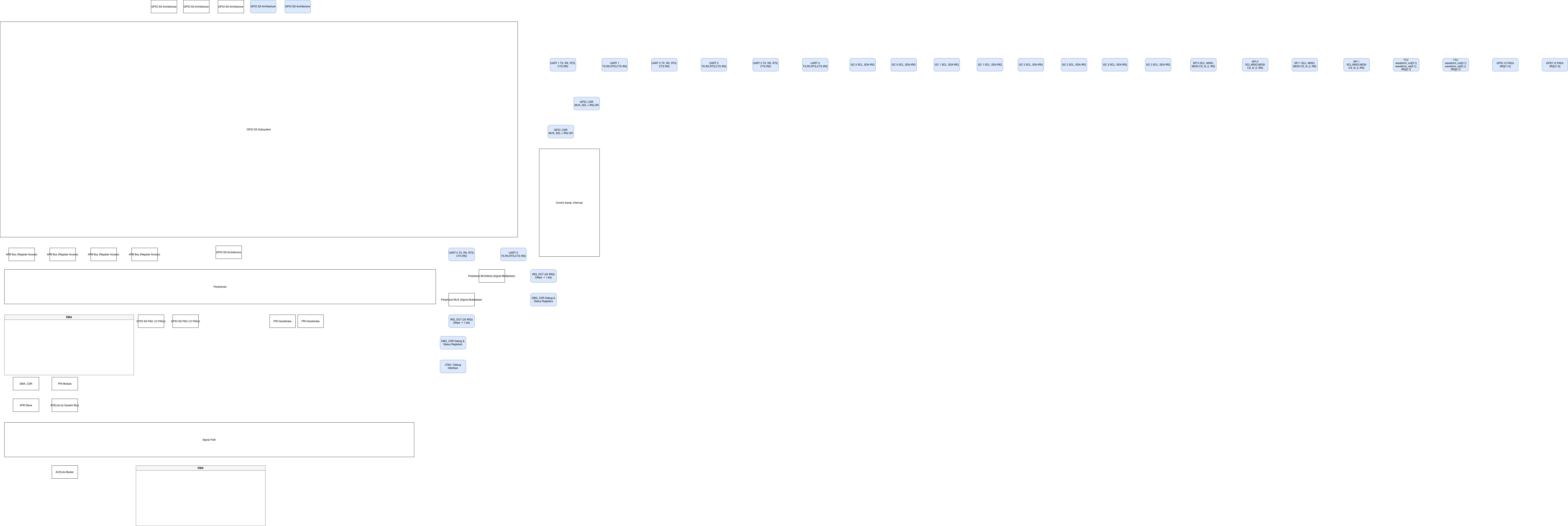
GPIO SS Peripheral Subsystem Architecture integrates four UART, four I2C, two SPI, and three TTC interfaces with 12 GPIO PADs through a centralized Peripheral MUX and GPIO_CSR.v control module. All 25 interrupts (UART, I2C, SPI, TTC, and GPIO) are ORed and routed via APB Bus register access and PRI Handshake logic to the system. The Peripheral MUX multiplexes signals from all peripherals to the GPIO SS PAD outputs, while GPIO_CSR.v manages MUX_SEL configuration and interrupt prioritization. This architecture enables flexible pin multiplexing and centralized interrupt handling, critical for reducing pin count and simplifying firmware interrupt management in resource-constrained SoCs. Fork this diagram to customize peripheral counts, modify interrupt prioritization schemes, or adapt the MUX topology for your specific silicon design. The modular design supports easy integration with ACELite Master and DMA subsystems for high-performance data transfers.
People also ask
How do you design a GPIO peripheral subsystem that multiplexes multiple UART, I2C, and SPI interfaces to a limited number of GPIO PADs?
This GPIO SS architecture uses a Peripheral MUX controlled by GPIO_CSR.v to route signals from four UART, four I2C, two SPI, and three TTC interfaces to 12 GPIO PADs. All 25 interrupts are ORed together and managed via APB register access, enabling flexible pin assignment and centralized interrupt prioritization in resource-constrained SoCs.
- Domain:
- Electrical Engineering
- Audience:
- embedded systems engineers designing GPIO peripheral subsystems and SoC architectures
Generated by Diagrams.so — AI architecture diagram generator with native Draw.io output. Fork this diagram, remix it, or download as .drawio, PNG, or SVG.